Team:EPF-Lausanne/ Microfluidics
From 2008.igem.org
| Home | The Team | The Project | Parts | 2-step PCR | Microfluidics | Modeling | Notebook |
|---|
Contents |
Methods
Chip design and functionality
The Chip we use was designed to meet the needs of our experiment: the device needs to provide a matrix devided into chambers where cells can grow. These chambers are connected by channels that will allow cell-cell, or in our case chamber-chamber,communication. The design that reflects best these aspects is the following:
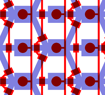
On this picture, the flow layer is represented in blue. This layer will contain all solutions and cells involved in the experiment. In red, the control layer is used to close and open the valves controlling the inlets and outlets of the flow layer.
Here is a zoom on one element of the design. The square chambers are overlaid by circular buttons. The Valves controlling the connection between two adjacent chambers also appear. One can observe the 3-to-1 connection pattern of the chip: every other cell receives an input from 1 other chambers, and the other from 3 chamber. This particular geometry is traduced in the modeling of our circuit.
A set of vertical valves between the chamber columns allows to control the communication between two adjacent rows. This way, we can control the moment when quorum-sensing molecules from one column are free to signal to the following column. Practically, this will allow us to wait a sufficient amount of time before the response of a given column chamber is computed by the cells and is ready to be received by the following column.
The valves are designed in such a way that they can be sequentially opened, using a minimum amount of inlets (for this reason, they are connected 2 by 2 which reduces the control inlets to 2 channels). There is also a set of circular buttons that, when activated, allow to trap the cells under their surface and circulate the surrounding medium.
All in all, the experiment will be conducted in the following order: the chip will be filled with cells containing our engineered plasmids. The buttons will then be closed and the medium circulated to eliminate cells that are not in chambers. Then, the signal in the first column will be initiated by addition of quorum-sensing molecules. Some time will be given to the cells to produce a response. Once there is production of response signal, the valves that control the connection to the following column will be opened. The 2nd column will now produce a response after some time, and again, the 2-3 connection is opened, and so on until the signal can run across the whole chip and cells in each column produce a response.
Physical characteristics of the chip
- the chambers are 300µm wide
- flow layer channels are 100µm wide
- control channels are 30µm wide when they need to cross flow layer structures without making a valve
- buttons have a 90µm radius
The ending of the inlets are opened to the exterior by punching wholes after the PDMS is solidified.
These control lines are filled with water. When sufficient pressure is applied on them, it causes the membrane separating the control and the flow layer to bend in such a way that the flow layer is closed. This allows a precise control of what enters the chip at a given time.
Once the design is prepared, it is transfered on a chrome mask by laser lithography and so on to obtain the corresponding wafers. This process is described in the following sections.
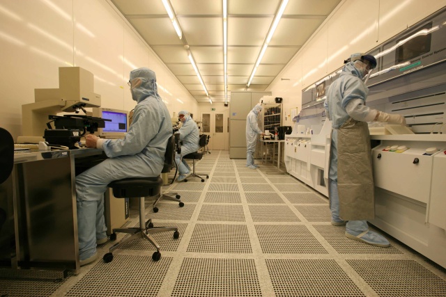
Molds fabrication - Clean room
Molds were fabricated at the [http://cmi.epfl.ch Center of MicroNanoTechnology at EPFL (CMI)] on silicon wafers. The flow wafers were coated with the AZ9260 positive resist at a thickness of 8um and the control wafers were coated with SU-8 negative photoresist at a thickness of 10um. SU-8 has the advantage to be more resistant and more stable than the positive resist. But, AZ9260 has the advantage that it can be rounded when baked and this property allows to have a better closing ability of the flow channels by the control valves.
On the meantime, two glass masks corresponding to each layer of the design (flow and control) were written using a laser pattern generator (Heidelberg DWL200). The photoresist was then removed by a standard developer, the chromium was removed on the Chr etching bench and the masks were finally cleaned in a hot bath of 1165 remover.
The masks were used to expose the corresponding wafers. Wafers were then baked slowly up to 100°C and developed with PGMEA and 2-propanol. For the positive resist (AZ9260), an additional bake was performed for 20 min at 160°C in order to round the edges of the flow channels.
PDMS chip fabrication
Once the wafers are ready, they are used as molds for PDMS (poly(dimethylsiloxane)). The designed chip has two layers: flow level, where the cells will ultimately grow and control layer, used to close and open certain valves by putting under pressure the thin membrane between the control and the flow layers.
As both layers serve different purposes, their fabrication also differs.
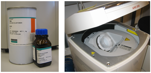
The production of the PDMS chip is performed as follows: The PDMS mix for control (C) and flow (F) layers is prepared separately. C-layer PDMS is a 5:1 mix of silicone and silicone curing agent. F-layer is a 20:1 mixture. Once the correct proportions have been measured, the mix is placed in a mixing defoaming machine that mixes the silicone and the curing agent in a homogeneous substance.
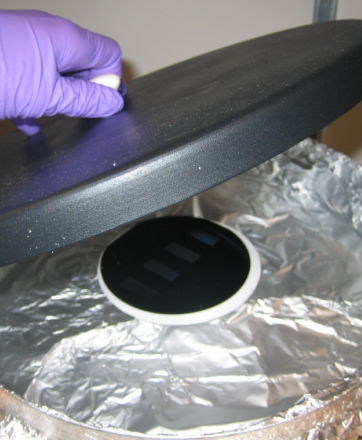
The liquid C-layer PDMS is casted directly on the wafer and set in a vacuum pump to eliminate any bubbles. The F-layer PDMS needs to form a very thin film over the wafer, so a spin coat machine is used.
Once both wafers are cast with PDMS, they are placed at 80°C for exactly 30 min. After the baking time, the PDMS from C-layer is solid and can be cut out from the wafer.
We now have two distinct layers that need to be aligned with each other. This process is done manually under a microscope.
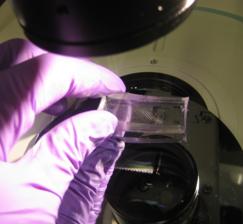
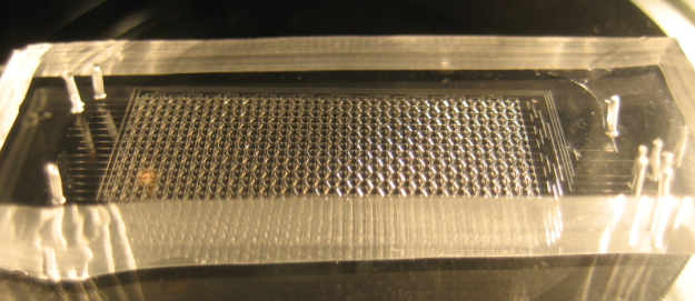
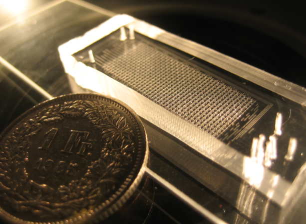
Once the chips are aligned, they are baked again at 80°C for 90 minutes. After this final bake, the C and F layers are tightly bound together. They can be easily detached from the wafer and put on a glass film for use in experiment. Again, if needed, additional wholes are punched. In the end the result is impressive!
Setup of the Experiment
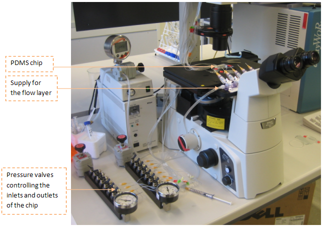
The product of the previous fabrication process can now be used in the experiment. The setup is the following:
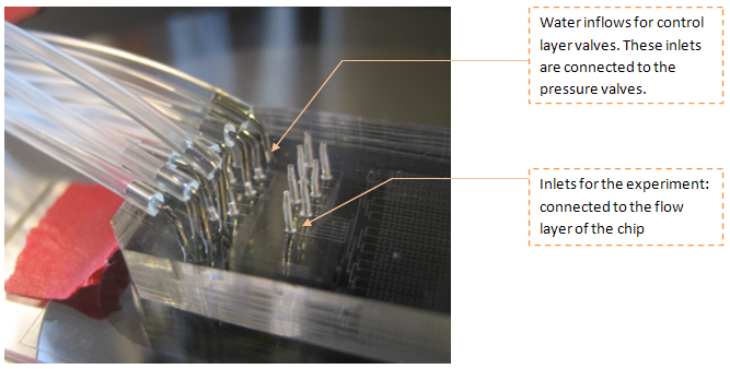
The connections with the chip are done using thin tubing and syringes. When the chip is ready to use the connections look like this:
Cell patterning on chip
MITOMI
S.Maerkl and S. Quake recently developed a high-throughput microfluidic platform capable of detecting low affinity transient binding events on the basis of the mechanically induced trapping of molecular interactions, called MITOMI (ref. 1). In the context of our project, we decided to use this technique to precisely look at the molecular interactions between our two key trans-activator molecules involved in quorum-sensing, RhlR and LuxR. We wanted to quantify the interactions of those two molecules, bounded or unbounded to their specific AHLs, with the sequences of the p(rhl) and p(lux) promoters. MITOMI is a good way to precisely characterize promoters and define cross-talks levels.
For detailed protocols, have a look at the Notebook.
Results
Chip functionality
We conducted several experiments with cells containing a plasmid with RFP under TetR-inducible promoter in order to characterize it. An overnight culture of RFP-cells was diluted in 1.5 mL of LB and loaded on chip.
The first column of the chip was also continuously flowed with TetR [0.2 mM] for diffusion on chip. We expected to observe the onset of RFP fluorescence when the trigger concentration of TetR would be reached.
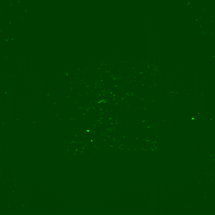
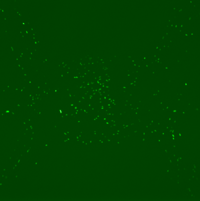
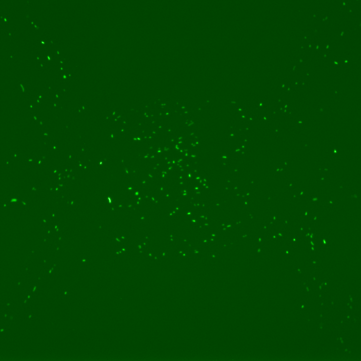
However, the results obtained revealed several dysfunctionalities of the chip. In most of the chambers, the cells had difficulties to grow and, overall, RFP expression in these chambers diminished with time. The number of cells also decreased until it reached a 'constant' population size (this is however hard to assess since the experiment time was ~2 hours). This is illustrated by the following set of pictures, where one can clearly see that between t0 and t1 the number of cells in the chamber drops dramatically but then stays constant. RFP fluorescence also decreases.
We believe that this might be due to several factors including the small amount of medium available to cells to survive and the high concentration of TetR used to initiate the experiment. This makes the readout of our results very complicated as the RFP signal decreases due to loss of cell activity in general. In these circumstances it is impossible to monitor the expression of RFP in response to TetR stimulation as the cells are in distress.
However, for some individual positions in the chip, we recorded a response consistent with our expectations: we can observe the increase of RFP expression even if the population of cells decreases in time. This might suggest that the experiment actually worked and these cells respond to a certain concentration of TetR as shown by the following pictures.
Cell patterning
MITOMI
Discussion
Reference
[http://www.ncbi.nlm.nih.gov/pubmed/17218526?ordinalpos=3&itool=EntrezSystem2.PEntrez.Pubmed.Pubmed_ResultsPanel.Pubmed_DefaultReportPanel.Pubmed_RVDocSum] Maerkl SJ, Quake SR. A systems approach to measuring the binding energy landscapes of transcription factors. Science. 2007 Jan 12;315(5809):233-7.
| Home | The Team | The Project | Parts | 2-step PCR | Microfluidics | Modeling | Notebook |
|---|
 "
"

